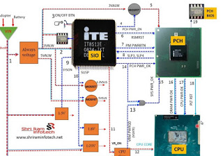
In the absence of any power supply (no battery and adapter) system is powered by 3V Battery to CMOS circuits to create VCCRTC which provide power to Southbridge RTC circuit to maintain internal communication time.

CMOS levels measured on RTC circuit with signals VCCRTC-DCPRTC # / RTCRST # / SRTCRST #. 3v source voltage is apply to 32.768KHz RTC Circuit of South bridge chip to save time system.
The battery or power adapter apply to system which is usually above 10.8v normally 19V DC on adapter and 10.8v-14.8v on battery is generated V+ or main B+ by two mosfet through system operated by charging ic
When adapter and battery creates a common supply at B+ , standby ic (ie 51125 ,max8734 hold 3.3v and 5v supply system) genrate 3.3v always to EC(kbc ic) (typically 3.3V power supply linear current 0.08A known as standby power).
Standby voltage supply EC (AVCC / VCC0 3.3v) and CMOS RTC source (32.768kHz 3.3V RTCVCC) and reset voltage (3.3V EC_RST # / ECRST # / WRST # / VCC_POR / VCC1_RST #) after read (BIOS) programming (oscillators can measure the waveform) system is ready to boot state.
If EC detect power adapter (charger IC good signal conversion ACOK ACIN / AD_IN / AC_IN / RI2 / WUI1 / GPD1 / ACAV_IN), will automatically send a signal to power standby ic to launch standby voltage (VCCSUS3_3, V5REF_SUS), and then EC signal sent to South chip called "RSMRST #" (3.3V).
Note:If South standby voltages are normal and no ACOK signal EC that's mean system on battery mode no ac adapter detected , then EC should receive signal from on/off switch to generate ,this is only to save electricity current from 0.02 to 0.03.
When you press the switch ON / OFF, EC received signal from switch (connected to the EC name GPIO03 / GPIO06 PWUREQ # / GPC7 / PWR_SW # - ASUS / TMRI0 / WUI2 / GPC4 / EC_GPXIOD3 / KBC_PWRBTN #) to send one High signal - PWRBTN to Southbridge control switch (COVER_SW # / LID_SW #).
When southbridge get PWRBTN # signal it sends signals SLP_S5 EC #, SLP_S4 #, # SLP_S3, SLP_S5 / S4 # conducted using the following feeds: (1)3.3VSUS(2)open source EC RAM (DDR1 0.05A 2.5 1.5V 1.8V DDR2 DDR3 V)(3) SLP_S3 # open source level after 3.3V_RUN, + 5_RUN,(4) south bridge power supply (1.5 V) bus-powered(5) (VCCP) 0.2A-0.3A 1.05V) graphics card offers Power(6)(0.5-0.7A 1.2V) VGA source VGPU_CORE
When above Voltages genrated EC Received signal OK EC, then EC circuit to switch to open the CPU voltage (VCORE) to line up with the current 0.6A that have the CPU power, (can see lines around 0.3-0.5A). At this point, the entire voltage has been opened completely.
After the power supply is normal, EC release VR_ON VRM to CPU management chip to enable CPU_VCORE ,CPU power management chip detect good Vcore Voltage Level its genrate VRMPWRGD / SYS_PWROK / MEPWROK about 3.3V CPU good signal to PM and SB (HM for i series).
PM and SB generate CK_PWRGD(CL_PWRGD) to the CPU power management chip which is simultaneously combined with the signal from the circuit CLK_EN which allows Clock HD generation( pulse CLOCK_GEN is for 945 or less and for the HM55 Series # CLK_EN).
After sucessful clock genration EC gerate PM_PWROK (SB_PWROK 3.3V) south brige or HM, southbridge will signal (CPUPWRGD / PROCPWRGD / DRAMPWROK about 1.05V) cpu section.NOTE: the CPU voltage opened successfully, and also signaling system startup PLTRST # (3.3V) and PCIRST # (3.3V)
Northbridge Chip after getting PLTRST #, # CPURST signal (1.05V 0.7A) to the CPU, the CPU begins work boot completion.
CPU start solving ADS #, read and retrieve data from BIOS.
Initialize the memory stream consumes about 0.7-0.8A
Initialize the graphics line 0.9-1.1A consumption
Show LOGO
Peripheral display

Good post
ReplyDeleteLaptop ,Desktop ,Led/Lcd,Tablet Pc Chip Level Servicing Tutorials: Laptop Power Sequence >>>>> Download Now
ReplyDelete>>>>> Download Full
Laptop ,Desktop ,Led/Lcd,Tablet Pc Chip Level Servicing Tutorials: Laptop Power Sequence >>>>> Download LINK
>>>>> Download Now
Laptop ,Desktop ,Led/Lcd,Tablet Pc Chip Level Servicing Tutorials: Laptop Power Sequence >>>>> Download Full
>>>>> Download LINK
Good idea please download above to get virus
DeleteYour post is really amazing with lots of important points Thank you for sharing. I was really enjoying reading this article.
ReplyDeletemobile repairing course in Laxmi Nagar
mobile repairing course in Laxmi Nagar Delhi